An independent laboratory
Nanoparticle innovation in search of a cancer cure
Celebrating 36 years of innovation!
All profits support our research.
Learn more about our:
- Nanoparticle Therapies: Our Cancer Research
- Nanoparticle Technology for your Lab:
Nanoparticle Products for Imaging, Microscopy and Biodetection
Home of the original Nanogold®
VivoVist™ Ultimate X-ray Contrast for Micro CT
Finally– affordable xray contrast agent for micro CT of rats and larger studies!
Precision nanoparticles boost definition and detail.
-
Blood pool agent
-
Highest contrast of competitors
-
Lowest price – makes larger studies & rat imaging affordable
-
Low toxicity allows high concentrations
- Low viscosity – easy to inject
- Compatible with any CT or xray system
- Specifically loads tumors for study & enhancement of radiotherapy
Get a free sample — See the difference for yourself!
Halo-FluoroNanogold™ Correlative 2-in-1 probe for Cryo-EM
The missing link for cryo-EM!
Take your Halo labeling to the next level with our new, 2-in-1 reagent!
Create multiplexed, correlative probes… Tiny, covalently bound, visible under both light and electron microscopes!
Halo tag ligand, PLUS:
-
Alexa® fluorescent label
- Fluorescent labels are available in any Alexa® color
- Get the big picture- see your targets in the light microscope
- Check your labeling before EM
-
Nanogold® for visibility in cryo-EM!
- Available in 0.8, 1.4, 5 and 12 nm sizes for multiplexing
- Also available in Halo-Nanogold® (no fluorophore)
The ultimate tool for labeling proteins in live cells now available from Nanoprobes.
We create custom combinations, according to your needs!
Free consultation with one of our experts.

3-in-1 Triple Gold Halo tags from Nanoprobes: 3-in-1 labels with 1.4 nm Nanogold®, fluorescent Alexa® 594, and a HaloTag. Penetrate the nucleus and find your target!
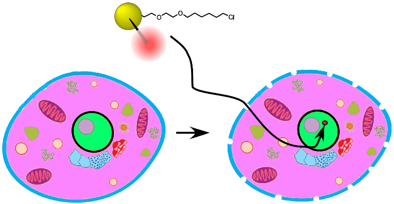
3-in-1 Triple Gold Halo tags carry a tiny, 1.4 nm Nanogold® probe, used to penetrate the nucleus and identify histones and their structure in live cells!
VivoVist™ Ultimate X-ray Contrast for Micro CT
Finally– affordable xray contrast agent for micro CT of rats and larger studies!
Precision nanoparticles boost definition and detail.
-
Blood pool agent
-
Highest contrast of competitors
-
Lowest price – makes larger studies & rat imaging affordable
-
Low toxicity allows high concentrations
- Low viscosity – easy to inject
- Compatible with any CT or xray system
- Specifically loads tumors for study & enhancement of radiotherapy
Get a free sample — See the difference for yourself!
Micro CT of live mouse vascular system – Incredible contrast with VivoVist™ -with a 14 hour blood half-life!
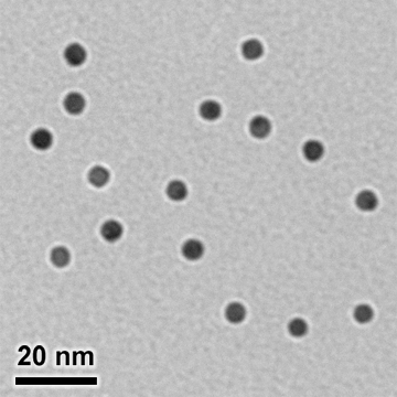
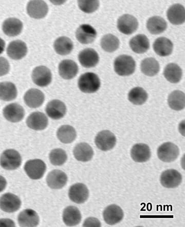

VivoVist™ Ultimate X-ray Contrast for Micro CT
Finally– affordable xray contrast agent for micro CT of rats and larger studies!
Precision nanoparticles boost definition and detail.
-
Blood pool agent
-
Highest contrast of competitors
-
Lowest price – makes larger studies & rat imaging affordable
-
Low toxicity allows high concentrations
- Low viscosity – easy to inject
- Compatible with any CT or xray system
- Specifically loads tumors for study & enhancement of radiotherapy
Get a free sample — See the difference for yourself!

Head of a live mouse imaged by microCT following intravenous VivoVist administration, using a Bruker SkyScan 1276 at 13 um voxels resolution. 3D image generated and analyzed with Horos v4.0.0. Brain vessels of 50 microns or smaller were resolvable. Image kindly provided by Dr. Sean Marrelli, Department of Neurology at the McGovern Medical School at UT Health (Houston, TX).
Our mission at Nanoprobes is to harness chemistry, biology and nanotechnology to engineer the most sensitive reagents and nanotechnology for detecting, locating and visualizing biological molecules.
Our unique gold nanoparticle labeling technology uses chemically cross-linked metal clusters and nanoparticles as labels.
Unlike conventional immunogold probes, in which colloidal gold particles are electrostatically adsorbed to antibodies and proteins, our gold nanoparticle labels are uncharged molecules which are cross-linked to specific sites on biomolecules. This gives our nanogold probes greater range and versatility than colloidal gold.
Our labels can be attached to any molecule with a reactive group — proteins, peptides, oligonucleotides, small molecules and lipids — for detection and localization. Other labels can be combined with our gold particle labels; our unique FluoroNanogold probes combine Nanogold® and fluorescein into a single probe for imaging a specimen both by fluorescence and electron microscopy. Our gold nanoparticles, including our Nanogold™ conjugates, and Nanogold™ labeling reagents, are formulated for use with electron microscopy (tem) as well as light microscopy, immunolabeling, x-ray contrast for EM, angiography, mammography and microCT, and for correlative and fluorescence microscopy imaging.
New probes can be engineered based on any fragment of a naturally occurring biomolecule, and the label can be positioned away from the binding site so it does not interfere with binding.
Our Nanogold® probes have been cited in over 250 publications, and are used in the laboratories of several Nobel Laureates.